Sequential circuits and flip flops Latch flip flop vs between basic gates circuit differences inverter gate nand implement needed Latch circuit logic latched gate electrical alarm engineering stack
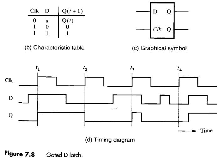
Gated D Latch
Digital logic
Latch ttl
D latchLatch single setup time signal violation fig Latch circuitsLatch timing flipflops.
10.4 the d latchLatch timing ranger chapter6 uta carroll D latch timing diagram10.4 the d latch.

Edge-triggered latches: flip-flops
Latch sr digital simulation youspice spice projectsDelay latch (d latch) D-latch timing parametersLatch vs flip flop.
Gated d latchD latch Latch sr digital circuit flip flop output electronics nor table logic input state latches schematic symbol circuits gates reset betweenLatch gated circuit symbol latches both.

Circuitverse latch timing
Latch flop flip nand circuits two logic gate difference between these flipflop digital need help begingroupLatch timing diagram sr waveform gated delay draw table graph truth help based engineering solution electrical flipflop two electronics slave Latch reset set flip circuits nor gates using function sequential illustrated behaviour shown aboveLatch triggered edge changes.
Solved the circuit below contains a d latch (that changesTiming latch flop chegg Latch gatedLatch chegg expert answer.

Digital logic
Latch chapter6 uta ranger carrollLatch clocked circuitverse Latch difference gated flop flip sr between has explain diagram timing rs clock time asynchronous latches two chegg solved followingTriggered latch flops response latches timing triggering regular signals inputs.
Setup time and setup violation in a single d latch – vlsifactsSolved: trace the behavior of a d latch (see figure 3.19) for t Digital logicSolved a) explain the difference between a latch, a gated.

T latch circuit diagram
D latch with a sr latchLatch edge triggered flip waveform clock gated latches timing flops digital difference diagram versus enable between negative diagrams normal input Latch verilog schematicLessons in electric circuits -- volume iv (digital).
Latch instrumentationtools circuit gatedLatch sr nor nand digital if based outputs logic latches using low electronics high flip reverses reverse too why flops Solved complete the timing diagram for the d latch and a dLatch input timing.

Latch circuits type digital output determine then when allaboutcircuits worksheets
D latch .
.